| Sign In | Join Free | My futurenowinc.com |
|
| Sign In | Join Free | My futurenowinc.com |
|
| Categories | PCBA SMT |
|---|---|
| Brand Name: | Angel-tech |
| Model Number: | Impedance PCB for Electrical box |
| Certification: | RoHS,ISO9001、ISO14001、TL9000、TS16949 |
| Place of Origin: | China |
| MOQ: | 10pieces |
| Price: | negotiated |
| Payment Terms: | T/T, Western Union,paypal.credit card |
| Supply Ability: | 10000pcs/month |
| Delivery Time: | 7-15days/discuss |
| Packaging Details: | Standard package |
| Application: | Electrical box |
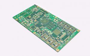
| Product Name: | Impedance PCB(Printed Circuit Board) for Electrical box |
| Characteristic: | High Reliability, Six-layer impedance boards |
| Base material: | FR4 |
| Layer(s): | 6 |
| Permittivity: | 4.3 |
| Thickness: | 1.6MM |
| Outer copper thickness: | 1oz |
| copper thickness(Inner): | 1oz |
| Mounting Type: | Immersion gold |
| Min Hole Diameter: | 0.2mm |
| Minimum line width: | 0.08mm |
| (MLI)Min Line Space: | 0.1MM |
| Stock: | In Stock |
| Company Info. |
| Angel Technology Electronics Co |
| Verified Supplier |
| View Contact Details |
| Product List |
Impedance PCB(Printed Circuit Board) for Electrical box with pcb manufacturing and assembly
Impedance PCB(Printed Circuit Board) for Electrical box pcb manufacturing service
Impedance PCB(Printed Circuit Board) for Electrical box Specification:
| Base material | FR4 | Layer(s) | 6 |
| Permittivity | 4.3 | Thickness | 1.6mm |
| Outer copper thickness | 1Oz | copper thickness(Inner) | 1oZ |
| Mounting Type | Immersion gold | Min Hole Diameter | 0.2mm |
| Minimum line width | 0.08mm | (MLI)Min Line Space | 0.1MM |
| Application | Electrical box | Characteristic | High Reliability, Six-layers impedance boards |
Impedance PCB(Printed Circuit Board) for Electrical box images:


Impedance PCB(Printed Circuit Board) for Electrical box shown details :


Our circuits boards range from double layers to 24 layers. The product types include ordinary boards, medium and high Tg boards, involving special processes such as semi-hole, bonding, impedance, blue glue, carbon oil, gold fingers, blind gongs, buried blind holes , Countersunk holes, etc.; surface treatment can be ordinary tin spray, lead-free tin spray, immersion gold, electro-nickel gold, electro-hard gold, QSP, immersion silver, immersion tin or composite processes, etc.. products are widely used in smart electronics, communications Technology, power technology, industrial control, security engineering, automotive industry, medical control and optoelectronic engineering and other fields.
Our PCB factory is fully qualified and has passed a series of certifications such as UL, ISO9001, ISO14001, ISO/TS16949, CQC and so on.
Quote Requirement:
*Gerber file of the bare PCB board.
*BOM (Bill of material) for assembly.
*To short the lead time, please kindly advise us if there is any acceptable components substitution.
*Testing Guide & Test Fixtures if necessary.
Welcome contact us for more informations,thank you!
| PCB Technical Specification | |
| Order Quantity | 1-500,000 |
| Layer | 1,2,4,6,up to 22 layers |
| Material | FR-4, glass epoxy, FR4 High Tg, Rohs compliant, Aluminum, Rogers, etc |
| PCB type | Rigid, flexible, rigid-flexible |
| Shape | Any shape: Rectangular,round,slots,cutouts,complex,irregular, etc |
| Max PCB dimensions | 20inch*20inch or 500mm*500mm |
| Thickness | 0.4~4.0mm |
| Thickness tolerance | ± 10% |
| Copper thickness | 1/2OZ 1OZ 2OZ 3OZ |
| Copper thickness tolerance | ± 0.25oz |
| Surface finish | HASL, Nickle, Imm Gold, Imm Tin, Imm Silver, OSP etc |
| Solder mask | Green, red, white, yellow, blue, black, etc |
| Silk screen | White, yellow, black, or negative, etc |
| Silk screen min line width | 0.006'' or 0.15mm |
| Min drill hole diameter | 0.01'',0.25mm.or 10 mil |
| Min trace/gap | 0.075mm or 3mil |
| PCB cutting | Shear,V-score,tab-routed |
PCB Assembly Capabilities | ||
| Item | Technical Parameter | |
| SMT Jointing Min. Space | 0201mm | |
| QFP Space | Pitch 0.3mm | |
| Min. Package | 0201 | |
| Min. Size | 2*2 inch(50*50mm) | |
| Max. Size | 14*22 inch(350*550mm) | |
| Placement Precision | ±0.01mm | |
| Placement Precision | QFP, SOP, PLCC, BGA | |
| Placement Capability | 0805, 0603, 0402, 0201 | |
| PCB Lead time (workday(s)) Normally | |||||
| Single, Double-sided | 4 layer | 6 layer | Over 8 layer | HDI | |
| Sample Lead time (Normal) | 5-6 | 6-7 | 7-8 | 10-12 | 10-12 |
| Sample Lead time (Faster) | 48-72 hours | 5 | 6 | 6-7 | 12 |
| Mass production lead time | 7-9 | 10-12 | 13-15 | 16 | 20 |
| PCB Assembly Lead time | |||||
| Sample Lead time | PCB Fab+Components preparation +PCBA=15 workdays | ||||
| Mass production lead time | PCB Fab+Components preparation +PCBA=21workdays | ||||

|