| Sign In | Join Free | My futurenowinc.com |
|
| Sign In | Join Free | My futurenowinc.com |
|
| Categories | High Density Interconnect PCB |
|---|---|
| Brand Name: | xingqiang |
| Model Number: | As Per Customer's Model |
| Certification: | ISO 9001 / RoHS /UL / IATF 16949 (automotive) |
| Place of Origin: | China |
| MOQ: | Sample,1 pc(5 square meters) |
| Price: | Based on Gerber Files |
| Payment Terms: | ,T/T,Western Union |
| Supply Ability: | 100000㎡/Month |
| Delivery Time: | NA |
| Product: | HDI PCB |
| Material: | High Tg FR-4 |
| Pcba Service: | Yes |
| Min. hole Size: | 0.1mm |
| Standard: | IPC-A-610E |
| Max Board Size: | 528*600mm |
| Surface Finishing: | OSP/ENIG/ENEPIG/Electroplated Gold |
| Minimum Line Space: | 3mil (0.075mm) |
| Quotation Condition: | Gerber Files or BOM |
| PCB Layers: | 2/4/6/8/10 or Customizable |
| Board Thinkness: | 1.6/1.2/1.0/0.8mm or Customized |
| Solder Ink Color: | Green,Red,Blue,White,Yellow,Black |
| Company Info. |
| Dongguan Xingqiang Circuit Board Technology Co., Ltd. |
| Verified Supplier |
| View Contact Details |
| Product List |
High-Density Interconnect PCB
HDI boards utilize advanced manufacturing techniques such as laser-drilled microvias, blind vias, and buried vias to connect different layers without occupying excessive surface area. This design allows for more components to be packed into a compact space, making it ideal for slim, lightweight products like smartphones, tablets, medical devices, and aerospace electronics.
Customized services(PCB or PCBA)
1. Gerber files (RS-274X),PCB thickness, ink color, surface
treatment process.
2. BOM (if PCBA or SMT process is needed)
3. Impedance requirements & stack-up (if available)
4.Test requirements (TDR, network analyzer, etc.)
We’ll reply within 24 hours with a free quote, DFM report, and material recommendation.
Manufacturing process:

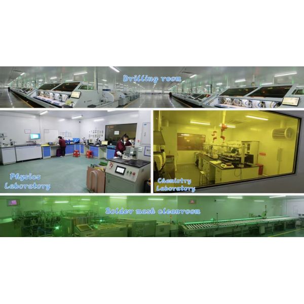
Factory showcase
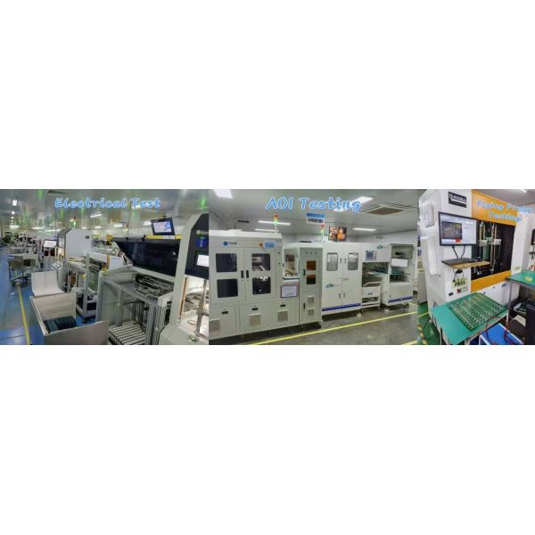
PCB Quality Testing
Certificates and Honors


|
