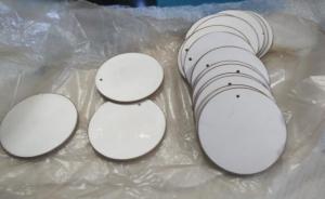
Precision Power Stoichiometric LiNbO3 Piezoelectric Wafer for Optoelectronic Applications

|
... is the key to success. Enter our Stoichiometric Lithium Niobate Wafer – a cutting - edge solution that will revolutionize your projects. Crafted with meticulous precision, our stoichiometric lithium niobate wafers boast an ideal 1:1 lithium - to -...
Hangzhou Freqcontrol Electronic Technology Ltd.
|
50um Ultra-Thin Piezoelectric Wafer LiTaO3 LT Film For Piezo Devices

|
...Piezoelectric Wafer LiTaO3 LT Film For Piezo Devices Lithium Tantalate (LT, LiTaO3) has unique properties, which as a material finds uses in Electro-Optical and Acousto-Optical applications. These can be : surface acoustic wave devices, bulk acoustic wave devices, piezo-electric transducers and piezoelectric......
ANHUI CRYSTRO CRYSTAL MATERIALS Co., Ltd.
|
8inch dia200mm LiNbO3 thin film Z-cut for Optoelectronic component

|
...Wafers LT & LN Wafer The basic principle of SAW devices is the generation of elastic surface waves from electrical signals and their reconversion. The substrate material is a piezoelectric crystal such quartz (SiO2), lithium tantalate (LiTaO3) or lithium niobate (LiNbO3). This are single crystal materials, which are cut out after the growth process with a defined orientation to a wafer......
SHANGHAI FAMOUS TRADE CO.,LTD
|
GaN Gallium Nitride Wafer High Electron Mobility RF Devices Optoelectronics And LEDs

|
... industries, owing to their unique material properties. With a wide bandgap, high electron mobility, and exceptional thermal stability, GaN wafers find applications in power electronics, RF devices, optoelectronics, and more. This abstract explores the...
SHANGHAI FAMOUS TRADE CO.,LTD
|
P44 Piezoelectric Disc Diameter 50mm 44Khz Wafer For Cleaning Transducer

|
... are exposed to pressure or stress. Examples of these materials are ceramics, also called piezoceramics , and crystals. Piezoelectric Ceramics (piezoceramics), such as Piezoelectric Ceramic Ring, Piezoelectric Ceramic Disc, Piezoelectric Ceramic Tube,...
Shenzhen Yujies Technology Co., Ltd.
|
N Type, InAs Wafer, 2”,Prime Grade,Epi Ready-Semiconductor Wafer Manufacturing
|
|
... wafer diameters range from 25.4 mm (1 inch) to 100 mm (6 inches) in size; wafers can be produced in various thicknesses and orientations with polished or unpolished sides and can include dopants. PAM-XIAMEN can produce wide range grades: prime ......
XIAMEN POWERWAY ADVANCED MATERIAL CO., LTD.
|
Optoelectronic Device SiC Wafer for Light Emitting Diodes

|
... material , with unique electrical properties and excellent thermal properties , compared to silicon wafer and GaAs wafer , SiC wafer is more suitable for high temperature and high power device application . SiC wafer can be supplied in diameter 2...
HENAN ZG INDUSTRIAL PRODUCTS CO.,LTD
|
20mm Wafer piezoelectric buzzer plate Piezo Ceramic Disc

|
... or tension is applied to the ceramic chip, charges of opposite polarity will be generated at the two ends of the ceramic chip and a current is generated through the circuit. This effect is called the piezoelectric effect....
TaiMi(Shenzhen) electronics technology Co.,ltd
|
P8 P4 Material Round Piezoelectric Ceramic Discs / Piezo Ceramic Disc 43 X 2mm

|
...piezoelectric ceramic wafer is electrical devices with a simple structure and light, with high sensitivity, no magnetic field spread without spillover, copper wire and magnets, low power consumption, less cost, easy mass production and the advantages of widely used. Suitable for ultrasonic and acoustic wave transmitting and receiving, piezoelectric......
Beijing Cheng-cheng Weiye Ultrasonic Science & Technology Co.,Ltd
|
LiNbO3 Lithium Niobate Wafer Piezoelectric For Optical Waveguides Mobile Phones

|
LiNbO3 Piezoelectric Crystals Description Lithium niobate (LN, LiNbO3) crystals are an important material for optical waveguides, mobile phones, piezoelectric sensors, optical modulators and various other linear and non-linear optical applications. Many ......
Nanjing Crylink Photonics Co.,Ltd
|
